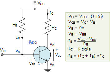
The steady state operation of a transistor depends a great deal on its base current, collector voltage, and collector current values and therefore, if the transistor is to operate correctly as a linear amplifier, it must be properly biased around its operating point.
Establishing the correct operating point requires the selection of bias resistors and load resistors to provide the appropriate input current and collector voltage conditions. The correct biasing point for a bipolar transistor, either NPN or PNP, generally lies somewhere between the two extremes of operation with respect to it being either “fully-ON” or “fully-OFF” along its DC load line. This central operating point is called the “Quiescent Operating Point”, or Q-point for short.
When a bipolar transistor is biased so that the Q-point is near the middle of its operating range, that is approximately halfway between cut-off and saturation, it is said to be operating as a Class-A amplifier. This mode of operation allows the output voltage to increase and decrease around the amplifiers Q-point without distortion as the input signal swings through one complete cycle. In other words, the output is available for the full 360o of the input cycle.
So how do we set this Q-point biasing of a transistor? – The correct biasing of the transistor is achieved using a process known commonly as Base Bias.
But before we start looking at the possible different transistor biasing arrangements, lets first remind ourselves of a basic single transistor circuit along with its voltages and currents as shown on the left.
The function of the “DC Bias level” is to correctly set the transistors Q-point by setting its Collector current ( IC ) to a constant and steady state value without any external input signal applied to the transistors Base.
This steady-state or DC operating point is set by the values of the circuits DC supply voltage ( Vcc ) and the value of any biasing resistors connected the transistors Base terminal.
Since the transistors Base bias currents are steady-state DC currents, the appropriate use of coupling and bypass capacitors will help block any biasing currents from other transistor stage affecting the bias conditions of the next. Base bias networks can be used for Common-base (CB), common-collector (CC) or common-emitter (CE) transistor configurations. In this simple transistor biasing tutorial we will look at the different biasing arrangements available for a Common Emitter Amplifier.
Base Biasing a Common Emitter Amplifier
One of the most frequently used biasing circuits for a transistor circuit is with the self-biasing of the emitter-bias circuit were one or more biasing resistors are used to set up the initial DC values for the three transistor currents, ( IB ), ( IC ) and ( IE ).
The two most common forms of bipolar transistor biasing are: Beta Dependent and Beta Independent. Transistor bias voltages are largely dependent on transistor beta, ( β ) so the biasing set up for one transistor may not necessarily be the same for another transistor as their beta values may be different. Transistor biasing can be achieved either by using a single feed back resistor or by using a simple voltage divider network to provide the required biasing voltage.
The following are five examples of transistor Base bias configurations from a single supply ( Vcc ).
Fixed Base Biasing a Transistor

The circuit shown is called as a “fixed base bias circuit”, because the transistors base current, IB remains constant for given values of Vcc, and therefore the transistors operating point must also remain fixed. This two resistor biasing network is used to establish the initial operating region of the transistor using a fixed current bias.
This type of transistor biasing arrangement is also beta dependent biasing as the steady-state condition of operation is a function of the transistors beta β value, so the biasing point will vary over a wide range for transistors of the same type as the characteristics of the transistors will not be exactly the same.
The emitter diode of the transistor is forward biased by applying the required positive base bias voltage via the current limiting resistor RB. Assuming a standard bipolar transistor, the forward base-emitter voltage drop would be 0.7V. Then the value of RB is simply: (VCC – VBE)/IB where IB is defined as IC/β.
With this single resistor type of biasing arrangement the biasing voltages and currents do not remain stable during transistor operation and can vary enormously. Also the operating temperature of the transistor can adversely effect the operating point.
Collector Feedback Biasing a Transistor

This self biasing collector feedback configuration is another beta dependent biasing method which requires two resistors to provide the necessary DC bias for the transistor. The collector to base feedback configuration ensures that the transistor is always biased in the active region regardless of the value of Beta (β). The DC base bias voltage is derived from the collector voltage VC, thus providing good stability.
In this circuit, the base bias resistor, RB is connected to the transistors collector C, instead of to the supply voltage rail, Vcc. Now if the collector current increases, the collector voltage drops, reducing the base drive and thereby automatically reducing the collector current to keep the transistors Q-point fixed. Therefore this method of collector feedback biasing produces negative feedback round the transistor as there is a direct feedback from the output terminal to the input terminal via resistor, RB.
Since the biasing voltage is derived from the voltage drop across the load resistor, RL, if the load current increases there will be a larger voltage drop across RL, and a corresponding reduced collector voltage, VC. This effect will cause a corresponding drop in the base current, IB which in turn, brings IC back to normal.
The opposite reaction will also occur when the transistors collector current reduces. Then this method of biasing is called self-biasing with the transistors stability using this type of feedback bias network being generally good for most amplifier designs.
Dual Feedback Transistor Biasing

Adding an additional resistor to the base bias network of the previous configuration improves stability even more with respect to variations in Beta, ( β ) by increasing the current flowing through the base biasing resistors.
The current flowing through RB1 is generally set at a value equal to about 10% of collector current, IC. Obviously it must also be greater than the base current required for the minimum value of Beta, β.
One of the advantages of this type of self biasing configuration is that the two resistors provide both automatic biasing and Rƒ feedback at the same time.
Transistor Biasing with Emitter Feedback

This type of transistor biasing configuration, often called self-emitter biasing, uses both emitter and base-collector feedback to stabilize the collector current even further. This is because resistors RB1 and RE as well as the base-emitter junction of the transistor are all effectively connected in series with the supply voltage, VCC.
The downside of this emitter feedback configuration is that it reduces the output gain due to the base resistor connection. The collector voltage determines the current flowing through the feedback resistor, RB1 producing what is called “degenerative feedback”.
The current flowing from the emitter, IE (which is a combination of IC + IB) causes a voltage drop to appear across RE in such a direction, that it reverse biases the base-emitter junction.
So if the emitter current increases, due to an increase in collector current, voltage drop I*RE also increases. Since the polarity of this voltage reverse biases the base-emitter junction, IB automatically decrease. Therefore the emitter current increase less than it would have done had there been no self biasing resistor.
Generally, resistor values are set so that the voltage dropped across the emitter resistor RE is approximately 10% of VCC and the current flowing through resistor RB1 is 10% of the collector current IC.
Thus this type of transistor biasing configuration works best at relatively low power supply voltages.
Voltage Divider Transistor Biasing

Here the common emitter transistor configuration is biased using a voltage divider network to increase stability. The name of this biasing configuration comes from the fact that the two resistors RB1 and RB2 form a voltage or potential divider network across the supply with their center point junction connected the transistors base terminal as shown.
This voltage divider biasing configuration is the most widely used transistor biasing method. The emitter diode of the transistor is forward biased by the voltage value developed across resistor RB2. Also, voltage divider network biasing makes the transistor circuit independent of changes in beta as the biasing voltages set at the transistors base, emitter, and collector terminals are not dependant on external circuit values.
To calculate the voltage developed across resistor RB2 and therefore the voltage applied to the base terminal we simply use the voltage divider formula for resistors in series.
Generally the voltage drop across resistor RB2 is much less than for resistor RB1. Clearly the transistors base voltage VB with respect to ground, will be equal to the voltage across RB2.
The amount of biasing current flowing through resistor RB2 is generally set to 10 times the value of the required base current IB so that it is sufficiently high enough to have no effect on the voltage divider current or changes in Beta.
The goal of Transistor Biasing is to establish a known quiescent operating point, or Q-point for the bipolar transistor to work efficiently and produce an undistorted output signal. Correct DC biasing of the transistor also establishes its initial AC operating region with practical biasing circuits using either a two or four-resistor bias network.
In bipolar transistor circuits, the Q-point is represented by ( VCE, IC ) for the NPN transistors or ( VEC, IC ) for PNP transistors. The stability of the base bias network and therefore the Q-point is generally assessed by considering the collector current as a function of both Beta (β) and temperature.
Here we have looked briefly at five different configurations for “biasing a transistor” using resistive networks. But we can also bias a transistor using either silicon diodes, zener diodes or active networks all connected to the transistors base terminal. We could also correctly bias the transistor from a dual voltage power supply if so wished.